Equipped with innovative, self-developed intelligent inspection software, the system enables high-speed 3D inspection. It can inspect components such as BGA, POP, LGA, QFP, CSP, CHIP, QFN, DIP through-hole components, IGBT, and others. The system can detect defects including missing components, misalignment, solder bridging, open solder joints, insufficient solder, voids, and tombstone effects.

Unique 3D/CT reconstruction technology enables inspection at speeds as fast as < 2 s per FOV

Innovative in-house developed algorithms achieve high-precision detection of defects such as open solder joints, voids, and DIP fill rate issues

Equipped with a three-layer gantry structure driven by linear motors and grating scales, enabling high-speed CT scanning

Flexible combination of projection numbers and resolution to meet inspection requirements for various scenarios
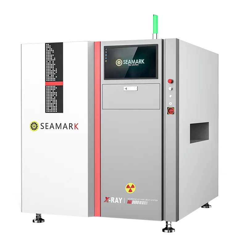
| Model | AXI9000 | |
|---|---|---|
| X-Ray Tube | Type | Reflection-sealed micro-focus X-ray source (optional) |
| Voltage Range | 50-130KV | |
| Current Range | 0-500 μA | |
| Maximum Output Power | 65W | |
| Flat Panel Detector | Type | Flat panel detector (optional) |
| Pixel Matrix | 1536×1536 | |
| Field of View (FOV) | 154mm×154mm | |
| Resolution | 5.0Lp/mm | |
| mage Frame Rate (1×1) | 30fps | |
| A/D Conversion | 16bits | |
| Equipment Specifications | X-Ray Leakage | <0.5μSv/hr |
| Air Pressure | 0.45~0.65MPa | |
| Input Power | 220V 10A 50-60HZ | |
| Control System | Professional GPU imaging workstation | |
| Dimensions | L1630mm×W1950mm×H1600mm | |
| Net Weight | 4000KG | |
| PCB Inspection | PCB Size | 50×50 - 610×510mm |
| CT Resolution | 6–50 μm/pixel (3 μm optional) | |
| PCB Thickness | 0.5mm-10mm | |
| PCB Height | Top ≤ 50 mm, Bottom ≤ 40 mm |


 EN
EN
 es
es  ko
ko  de
de  it
it  pt
pt  th
th  ar
ar  pl
pl  vi
vi  tr
tr  ru
ru


