Leakage dose < 1μSv/h, fully compliant with CE, FDA, and International Radiation Safety Standards.
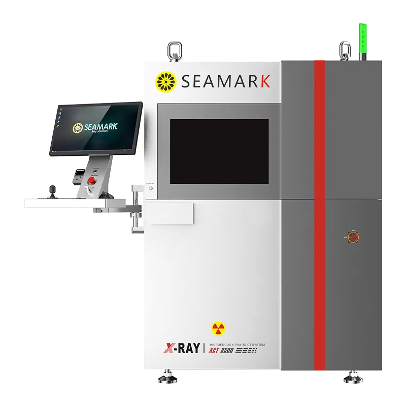
The XCT8500 3D CT X-Ray Inspection for Semiconductor, IGBT & Complex BGA Void Analysis consists of a X-ray source, detector, scanning system, image reconstruction and analysis system. It can achieve inspection methods such as 2D/3D/CT, and is suitable for quality inspection, 3D measurement, and non-destructive analysis. Characterizing the micro-scale features of the internal structure of the sample, combined with qualitative and quantitative analysis software to achieve multi-angle measurement and analysis of the sample, as well as automatic determination of OK/NG conditions, and to provide effective data for product quality inspection.
It can be used for electronic component soldering quality inspection, BGA component, integrated circuit (IC) and its binding line inspection, semiconductor packaging inspection and internal connection, electronic power (IGBT) module inspection, and Wafer defect inspection (WLCSP).Including missing parts, deviation, tin connection,contamination, faulty soldering, component foot warping, voids, pillow effect, and other soldering abnormalities.
![]()
Ensures the inspection area remains centered in the image even when the detector is tilted or rotated.

Combines image fusion and super-resolution technologies to clearly highlight defect features.

Geometric magnification up to 2500×, with defect detection capability below 1 μm.

Real-time radiation monitoring, safety interlock system, and automatic X-ray source shutdown during idle states.
XCT8500 adopts open micro-focus transmission X-ray source, the inspection ability can reach 0.5μm. It can realize 2D/3D/CT and other inspection methods, and is suitable for quality inspection,three-dimensional measurement and non- destructive analysis.

| Model | XCT8500 | |
|---|---|---|
| X-ray Tube | Tube Type | Open-type microfocus transmission X-ray source |
| Tube Voltage Range | 20-160KV | |
| Tube Current Range | 0.01mA~1.0mA | |
| Maximum Tube Power | 64W | |
| Maximum Target Power | 15W | |
| Minimum FOD (Focus-to-Object Distance) | <300μm | |
| Microfocus Spot Size | 2μm | |
| Minimum Detectable Defect Size | ≤1μm | |
| Flat Panel Detector | Detector Type | Amorphous silicon flat panel detector |
| Pixel Matrix | 1536x1536 | |
| Field of View (FOV) | 154mmx154mm | |
| Spatial Resolution | 5.0Lp/mm | |
| Image Frame Rate (1×1 binning) | 30fps | |
| A/D Conversion | 16bits | |
| 3D / CT Parameters (Optional) | CT Scanning Modes | Supports both ACT and PCT modes |
| 3D Visualization | Professional 3D visualization and analysis software | |
| System Specifications | Sample Stage Size | 645mmx635mm |
| Maximum Inspection Area | 500mmx500mm | |
| Maximum Geometric Magnification | 2000X | |
| Power Supply | 220V 10A 50-60HZ | |
| Control System | DELL OptiPlex 7000 MT 12th Gen i9 graphics workstation (or equivalent or higher-performance workstation) | |
| Overall Dimensions | L1500mmxW1650mmxH2250mm | |
| Net Weight | 3210KG |


 EN
EN
 es
es  ko
ko  de
de  it
it  pt
pt  th
th  ar
ar  pl
pl  vi
vi  tr
tr  ru
ru


