
A BGA footprint prepared at a PCB rework station is ready for a replacement component when its lands are intact, sufficiently level for the specified deposition process, clean and verified against the board documentation. The objective is not to expose bright bare copper everywhere. Unnecessary scraping or repeated wicking can remove useful finish and damage the very attachment surfaces the replacement needs.
Good site preparation starts as soon as the old package is lifted. Inspect first, then select a controlled removal method for the actual solder condition. Treat the PCB rework station as part of a complete process that includes support, suitable tools, cleaning and an explicit inspection hold before placement.
An acceptable site has the expected land pattern, no unresolved damage and no loose material that could interfere with the new attachment. Some residual solder immediately after removal is normal. Its distribution can reveal uneven release, but appearance alone cannot establish what happened at every joint.
Photograph the site before redressing it. Record unusual solder accumulations, missing features, lifted mask or fragments of package and adhesive. Cleaning can erase clues about the removal process, so initial documentation helps distinguish pre-existing damage from damage introduced later.
Compare the observed PCB land pattern with the board fabrication data and the component's package ball map. An intentionally absent solder ball does not, by itself, establish whether the corresponding PCB land should be present. Investigate discrepancies against both drawings before adding solder or accepting a missing land.
Plan the desired final surface with the replacement process in mind. A process using controlled solder paste deposition has different preparation considerations from an approved flux-only attachment. Site preparation should produce the defined condition for that process, rather than chase an arbitrary visual ideal.
Before touching the site, confirm the assembly is stable, accessible and suitably supported. If it rocks or flexes when the tool approaches, correct the setup first. Stable support makes light, controlled contact possible and improves inspection consistency.
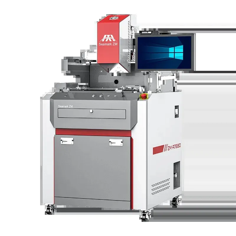
Remove excess solder with enough controlled heat to let the chosen method work without forcing the tool across solid material. A too-small or poorly coupled tip may encourage longer dwell and higher pressure; an oversized tool may expose neighboring features unnecessarily. Match the tool to the land geometry and thermal demand.
Use compatible flux where the process calls for it. Flux supports wetting and solder transfer, but adding more does not compensate for a contaminated tool, insufficient heating or damaged lands. Keep consumables identified and follow their handling instructions.
During contact removal, avoid dragging braid or a tip against solder that has solidified. If the tool sticks, restore appropriate heat through the controlled method before separating it. Pulling upward can transfer force directly to a land or trace.
Work in limited passes and inspect between them. Repeatedly traversing the entire array can accumulate thermal and mechanical exposure without improving an already acceptable region. Stop when the specified residual-solder condition has been reached; the last visible trace of solder is not automatically a defect.
For component rework and board repair, keep package removal and site redressing as separate checkpoints. A package can lift cleanly while the subsequent cleanup damages the PCB. Recording the site condition at both stages helps identify which operation needs adjustment.
Solder wick is useful when it can be applied with controlled heat, contact and movement. Select suitable braid size and condition rather than pressing a wide, saturated section over a small array. Fresh material and an appropriate tip can improve transfer without increasing force.
Tips transfer heat directly and require a geometry that suits the task. Keep the working surface maintained and use a process-defined contact time. The temperature displayed by the iron does not establish the temperature of each PCB land, especially beside copper planes that carry heat away.
Contactless solder removal reduces direct tool contact with the lands, but it introduces other controls. The head gap, board flatness, heat delivery and extraction need to suit the assembly and material. A method described as contactless is not automatically harmless to solder mask or nearby components.
Method | Useful capability | Main control concern |
Solder wick | Accessible local solder transfer | Sticking, pressure and repeated dwell |
Controlled tip method | Direct thermal coupling | Tip geometry and local exposure |
Contactless removal | Reduced direct land contact | Gap, heating and extraction stability |
Choose a method based on the board and demonstrated result, not a blanket ranking. Fine lands, large thermal planes, local obstructions and required throughput can change the best option. A representative trial should include the site's condition after cleaning, rather than only the speed of solder removal.
When comparing BGA rework equipment, verify which site-preparation functions are actually included and which require separate tools. Optical alignment and package heating do not necessarily provide residual-solder extraction.
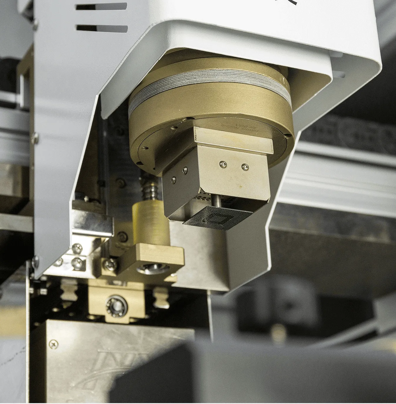
A lifted land may show an edge separating from the laminate, an altered level or a visible tear where a trace joins it. A missing land can leave exposed substrate. Use magnification and controlled lighting to distinguish these features from flux residue or normal finish variation.
Solder mask damage may appear as scratches, missing bridges or exposed conductor edges. Its significance depends on location and the assembly design. Damage between closely spaced lands can change the risk of bridging or contamination, so it should be assessed before solder deposition conceals it.
Do not probe aggressively to confirm a suspected lifted pad. Mechanical testing with an uncontrolled tool can turn a doubtful feature into definite damage. Escalate for the appropriate inspection and repair disposition instead.
Electrical checks can help establish continuity and unwanted connections on accessible nets. They do not prove adhesion strength, and a passing result does not automatically release a visibly damaged land for reuse. Likewise, a dark area is not sufficient evidence of burned laminate without further examination.
A repaired pad introduces another process boundary. Its geometry, attachment, electrical connection and ability to tolerate the next thermal cycle must be acceptable for the application. Do not assume that adding solder over a damaged feature restores the original structure.
Release the site only after cleaning, drying where required and inspection under the defined acceptance criteria. Confirm the land pattern, solder distribution, mask condition and absence of loose particles. Inspect nearby parts that could have shifted or collected debris during removal.
The cleaning method must match the flux and assembly materials. A solvent can spread contamination if it is used without effective removal, and residual liquid may remain beneath neighboring components. Follow the approved process rather than judging cleanliness solely by whether the board looks glossy.
Check flatness and access for the intended stencil or dispensing method. Residual adhesive, shields or protruding components can prevent correct seating even when the lands themselves are sound. Reconfirm orientation before bringing the replacement BGA into the work area.
Use a short recorded release checklist tied to the board identity. It should identify any repair disposition, confirm that the site has passed inspection, and authorize the next operation. This is more effective than relying on the next operator to notice a small defect after paste has been applied.
A suitable rework system supports repeatable placement, but it cannot compensate for an unacceptable footprint. Apply the same release discipline whether the next step is manual, semi-automatic or fully automatic.
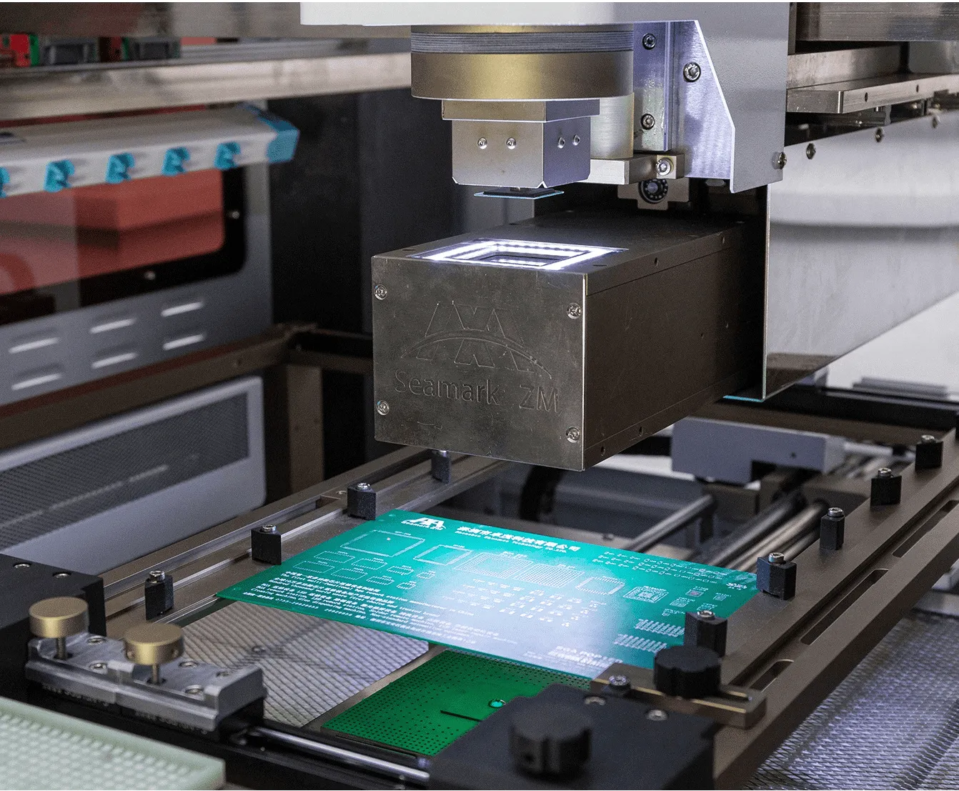
No. The required surface depends on the board finish and approved attachment process. Removing finish or copper to achieve a uniform color can damage an otherwise usable site.
Potential causes include sticking to solidified solder, excessive force or an already weakened land. Review heat transfer, tool condition and the board's prior damage rather than blaming the consumable alone.
No method is automatically safe on every board. Contactless removal reduces direct contact but still requires control of heating, working gap and material extraction.
Use the inspection and measurement tools specified for the product. Magnification, suitable lighting and appropriate electrical checks commonly complement the station, while specialized damage may require further evaluation.
Prepare the BGA site to a defined attachment condition with minimal necessary heat and force. Inspect before redressing, control each removal pass, and separate electrical continuity from mechanical integrity. Hold placement until the lands, mask, cleanliness and geometry have been accepted.
· IPC-7711C/7721C: Rework, Modification and Repair of Electronic Assemblies (Table of Contents)
· NASA / Jet Propulsion Laboratory: NASA Guidelines for BGA and DSBGA Selection and Application
 EN
 es
 ko
 de
 it
 pt
 th
 ar
 pl
 vi
 tr
 ru