
Press-fit connectors are widely used in automotive electronics, industrial control systems, telecommunications equipment, and other electronic assemblies that require reliable electrical connections. Unlike conventional soldered connectors, press-fit technology creates electrical and mechanical connections by inserting specially designed pins into plated through-holes on a printed circuit board (PCB).
Although press-fit assembly can eliminate soldering in the connector installation process, hidden defects may still occur during insertion. An X ray PCB inspection machine helps manufacturers examine internal connection structures, identify suspicious pin positions, and investigate potential PCB assembly issues without immediately destroying the sample.
This article explains common press-fit connector defects, how X ray PCB inspection supports quality control, and how manufacturers can select an appropriate inspection solution.
Press-fit connections depend on controlled mechanical interference between the connector pin and the plated through-hole. When the pin is inserted correctly, its compliant section deforms within the hole to establish electrical contact and mechanical retention.
However, insertion force, hole dimensions, pin geometry, PCB thickness, and material properties can all influence the final connection.
Common inspection challenges include:
Incorrect pin seating: Pins may be incompletely inserted or positioned unevenly.
Bent or displaced pins: Misalignment during insertion can affect the connection and potentially damage surrounding structures.
Plated through-hole damage: Excessive insertion force or unsuitable tolerances may damage the hole barrel or surrounding laminate.
Connector alignment problems: Uneven connector positioning may indicate an assembly issue.
Hidden structural irregularities: Internal connection features cannot always be assessed through conventional visual inspection.
An X-ray PCB inspection machine provides internal imaging that can help engineers investigate these issues. It is particularly useful when connector bodies, PCB layers, or neighboring components prevent direct visual access.
Nevertheless, X-ray inspection does not replace every verification method. Mechanical retention testing, electrical continuity testing, and destructive cross-section analysis may still be necessary to confirm specific connection requirements.
The ability to identify a defect depends on its physical characteristics, the imaging system, and the orientation of the inspected assembly.
A press-fit pin that does not reach its intended seating position may create an unreliable connection or fail to meet assembly specifications.
X-ray imaging can help engineers assess pin position relative to the PCB and connector geometry. Comparing inspected samples with known-good assemblies can make positional deviations easier to identify.
Pins may become bent or displaced when connector alignment is incorrect or insertion conditions are unsuitable. These problems can affect electrical contact and mechanical stability.
A suitable X-ray view can reveal abnormal pin orientation or positioning. However, overlapping structures may obscure some details, so multiple viewing angles or additional inspection methods may be required.
Press-fit assembly places mechanical stress on the plated through-hole. Excessive interference or unsuitable insertion conditions may damage the copper plating or surrounding PCB material.
An X-ray image may reveal certain structural abnormalities, but subtle cracks, plating damage, or internal material defects are not always reliably identifiable through conventional 2D imaging. Cross-section analysis may be required for confirmation.
Connector misalignment can create problems during subsequent assembly, mating, or mechanical integration. X-ray inspection can help assess the relationship between connector pins and PCB holes, particularly when the relevant structures are hidden.
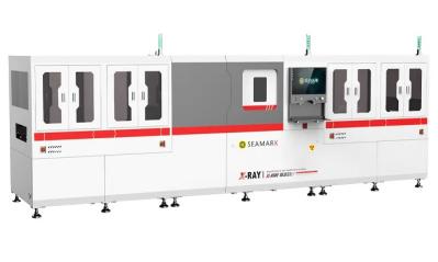
An X-ray PCB inspection machine uses penetrating X-rays to generate images based on differences in material absorption. Dense materials and different internal geometries produce varying image contrast, allowing engineers to examine features that are not visible from the outside.
For press-fit connector applications, the inspection process typically involves several steps.
First, the operator positions the PCB and selects an appropriate imaging orientation. The inspection settings are adjusted according to board thickness, connector materials, pin dimensions, and the required level of detail.
Next, the operator examines the resulting image to identify suspicious pin positions, irregular geometries, or other features relevant to the inspection criteria. Where necessary, additional projections are captured to reduce ambiguity caused by overlapping structures.
Finally, the findings are compared with engineering drawings, known-good samples, and applicable acceptance requirements.
For manufacturers performing offline inspection, this process provides flexibility for sample evaluation, production troubleshooting, incoming quality checks, and failure analysis. Boards can be examined at a separate workstation without requiring the inspection equipment to be integrated directly into the production line.
When evaluating an X-ray system, buyers should consider image resolution, magnification, sample size, imaging flexibility, software capabilities, and the ability to inspect representative connector assemblies.
Choosing between 2D X-ray and 3D computed tomography (CT) depends on the complexity of the connector structure and the evidence required.
| Evaluation factor | 2D X-ray inspection | 3D CT inspection |
|---|---|---|
| Image presentation | Two-dimensional projection | Reconstructed three-dimensional structure |
| Pin position assessment | Suitable for many routine checks | Provides additional spatial information |
| Overlapping structures | May complicate interpretation | Can help separate features by depth |
| Inspection workflow | Often faster for routine screening | Usually involves additional scanning and reconstruction |
| Detailed internal analysis | Depends on image quality and geometry | Useful for more complex internal structures |
A 2D system may be sufficient for routine pin-position checks and other clearly visible structural features. A CT-capable system may be more appropriate when overlapping pins, complex internal geometries, or detailed failure analysis make conventional projections insufficient.
Manufacturers should validate both approaches using representative samples rather than assuming that 3D imaging is necessary for every inspection task.
Before purchasing an inspection system, manufacturers should define their actual inspection requirements.
1. Identify the target defects. Determine whether the primary objective is checking pin seating, connector alignment, potential structural damage, or other internal features.
2. Prepare representative samples. Include known-good assemblies and samples with verified defects whenever possible.
3. Evaluate image quality. Confirm that the system can resolve the smallest features relevant to the application under realistic inspection conditions.
4. Assess workflow requirements. Consider PCB dimensions, daily inspection volume, sample handling, reporting, and traceability requirements.
5. Establish acceptance criteria. Use connector specifications, PCB manufacturing requirements, and customer quality standards to determine pass/fail conditions.
Yes. X-ray imaging can help identify abnormal pin positions and alignment issues when the relevant features are sufficiently visible. Inspection results should be compared with engineering specifications and reference samples.
Not by itself. X-ray provides structural information, while electrical continuity and other functional tests are needed to verify electrical performance.
Some structural defects may be visible, depending on their size, orientation, and the system's capabilities. Fine cracks or subtle plating damage may require destructive cross-section analysis or other suitable testing methods.
Yes. Offline inspection can support quality audits, sample testing, process troubleshooting, and failure analysis without requiring an inline inspection system.
Useful information includes PCB dimensions, connector types, pin geometry, target defects, sample images, production volume, and required acceptance criteria. Representative samples allow suppliers to evaluate whether the proposed equipment can meet the application requirements.
Press-fit connectors provide an alternative to soldered connections, but their hidden mechanical and electrical interfaces require appropriate quality verification. An X ray PCB inspection machine can help manufacturers examine pin seating, connector alignment, and selected internal structural features that conventional visual inspection cannot access.
The most suitable solution depends on the target defects, board geometry, image quality requirements, and production workflow. By validating inspection performance with representative samples and combining X-ray imaging with electrical or destructive testing when necessary, manufacturers can make more reliable quality-control decisions and select an appropriate PCB inspection system.
 EN
 es
 ko
 de
 it
 pt
 th
 ar
 pl
 vi
 tr
 ru