
Wire bonding remains an important interconnection technology in semiconductor packaging, connecting silicon dies to package leads or substrates through fine metal wires. However, defects such as wire deformation, unintended contact, and broken connections can affect package reliability and manufacturing yield. Because these wires are enclosed within semiconductor packages, conventional optical inspection cannot directly examine every internal feature.
Industrial X-ray imaging provides a non-destructive method for examining selected internal structures and identifying potential wire bonding abnormalities. With suitable imaging capabilities, an automated X-ray system can also support repeatable inspection workflows for semiconductor manufacturers. This guide explains common wire bond defects, X-ray inspection capabilities, and how to choose an appropriate inspection solution.
Wire bonds are typically made from fine gold, copper, or other conductive wires. Their dimensions, spacing, and geometry vary according to the package design and manufacturing process.
Several factors make wire bond inspection challenging:
Limited physical access: Bond wires are enclosed within the package and cannot be fully inspected using conventional external visual methods.
Fine internal structures: Small wire diameters and narrow spacing require appropriate image resolution and contrast.
Overlapping wire loops: Multiple wires may overlap in a two-dimensional projection, making individual features difficult to distinguish.
Potential hidden defects: Abnormal wire geometry or unintended contact may not be visible from the outside of the package.
Industrial X-ray imaging helps engineers examine internal wire arrangements without immediately opening or destroying the package. It is useful for quality investigations, process verification, and failure analysis when the target features can be resolved by the inspection system.
However, X-ray imaging does not automatically confirm the electrical integrity or mechanical strength of every wire bond. Complementary tests may be required to verify specific failure mechanisms.
Understanding the defect type helps manufacturers determine whether X-ray inspection is suitable and what imaging configuration may be required.
Wire sweep occurs when bond wires are displaced from their intended positions, potentially due to molding flow or other process-related forces. Excessive deformation may reduce wire spacing or create unintended contact between adjacent wires.
X-ray images can help engineers examine wire loop geometry and identify suspicious displacement. Comparing the inspected package with design references or known-good samples can support more consistent evaluation.
A broken wire may interrupt an electrical connection and cause package malfunction. Depending on the break location, wire orientation, and image quality, X-ray imaging may reveal an interrupted or abnormal wire path.
Nevertheless, very fine breaks may be difficult to distinguish from overlapping structures or low-contrast regions. Electrical testing and other failure-analysis techniques may be necessary to confirm the condition.
When adjacent wires become excessively close or touch, unintended electrical connections may occur. This risk is particularly important in packages containing dense wire bond arrangements.
X-ray inspection can help identify suspicious wire spacing and overlapping projections. Additional viewing angles or three-dimensional analysis may be useful when the apparent contact could be caused by projection overlap.
Wire loop height, shape, and routing influence package assembly and clearance. Abnormal loops may indicate bonding-process variation or potential interference with other internal structures.
By examining internal wire geometry, engineers can compare samples, investigate process deviations, and determine whether further analysis is necessary.
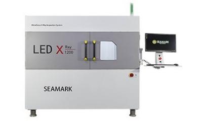
An X-ray inspection system generates images by measuring differences in X-ray transmission through materials and structures. The resulting contrast depends on factors such as material composition, thickness, geometry, detector performance, and imaging settings.
For semiconductor wire bond applications, an effective inspection process generally includes the following steps:
Define the inspection target. Identify whether the objective is to examine wire sweep, potential breaks, unintended contact, or other internal package features.
Select suitable imaging parameters. Adjust magnification, exposure, and imaging geometry according to the package and target feature.
Capture and evaluate images. Examine wire paths, spacing, and suspicious structural changes.
Compare reference samples. Use known-good packages and verified defect samples to support consistent interpretation.
Confirm uncertain findings. Apply electrical testing, microscopy, or destructive analysis when the image alone cannot establish the defect.
For applications involving complex wire arrangements, a system capable of capturing images from different angles can help reduce ambiguity caused by overlapping structures.
A three-dimensional CT-capable system may provide additional spatial information when two-dimensional images are insufficient. However, CT is not necessarily required for every wire bond inspection task. The decision should depend on the target defect, package geometry, inspection throughput, and required analytical detail.
An automated X-ray system may be appropriate when semiconductor manufacturers need repeatable inspection procedures, consistent image acquisition, and reduced dependence on manual operation.
Automation can support predefined inspection recipes, programmed imaging sequences, image processing, and result recording, depending on the equipment configuration. These functions may be particularly valuable when inspecting multiple package types or handling recurring quality-control tasks.
Before selecting an automated solution, manufacturers should evaluate several factors.
Inspection resolution: Confirm that the system can resolve the smallest wire features relevant to the application.
Repeatability: Test whether repeated inspections produce consistent images and classifications under defined conditions.
Throughput: Assess the time required for sample loading, image acquisition, processing, and review.
Software capabilities: Evaluate image comparison, measurement tools, reporting, and data storage according to actual requirements.
Integration requirements: Determine whether the equipment needs to communicate with existing quality management systems or production software.
For semiconductor manufacturers conducting sample analysis, process troubleshooting, or laboratory quality checks, offline inspection can provide a flexible approach without requiring the X-ray equipment to be integrated directly into the production line.
Equipment specifications alone cannot establish whether an inspection system is suitable for a particular semiconductor package. Manufacturers should conduct application-specific testing before making a purchasing decision.
Prepare representative packages, including known-good samples and verified defect samples where available. Define the smallest target feature, required image quality, inspection conditions, and criteria for classifying suspicious results.
During evaluation, examine whether the system can distinguish individual wires, reveal relevant geometric abnormalities, and produce repeatable results. If the application requires automated inspection, also assess recipe consistency, data recording, and the handling of false calls.
Document the results and identify situations where additional electrical or destructive testing remains necessary. This approach helps manufacturers establish realistic expectations and select an inspection solution based on demonstrated performance.
X-ray imaging may reveal broken wires or abnormal wire paths when the features are sufficiently visible. Very fine defects may require additional verification using electrical testing or other failure-analysis methods.
Potentially, yes. Suitability depends on the system's imaging range, resolution, software, sample handling, and available inspection recipes. Each package type should be validated before routine use.
Yes. Offline inspection is useful for sample evaluation, quality audits, process troubleshooting, and failure analysis when inspection can take place at a separate workstation.
CT may help when overlapping wires or complex internal structures make two-dimensional images difficult to interpret. Its additional scanning and reconstruction requirements should be weighed against the analytical benefits.
No. X-ray inspection provides structural information but does not independently guarantee electrical performance or mechanical bond strength. Appropriate electrical, mechanical, and reliability tests may still be required.
Semiconductor wire bond inspection requires careful evaluation of fine internal structures that are inaccessible to conventional external visual inspection. Industrial x ray imaging helps manufacturers examine wire geometry, investigate potential wire sweep, and identify suspicious internal features without immediately destroying the package.
For recurring inspection tasks, an automated x ray system may improve workflow consistency and support structured image analysis. Meanwhile, offline inspection provides a flexible option for sample evaluation and process investigation. By validating equipment with representative samples and combining X-ray imaging with complementary testing where necessary, semiconductor manufacturers can make better-informed decisions about inspection performance and package quality.
 EN
 es
 ko
 de
 it
 pt
 th
 ar
 pl
 vi
 tr
 ru