
Rigid-flex printed circuit boards (PCBs) combine rigid circuit sections with flexible circuits, allowing electronic products to accommodate compact spaces, complex geometries, and demanding mechanical requirements. They are commonly used in medical electronics, aerospace systems, automotive electronics, and portable devices. However, their multilayer structures and overlapping conductive features can make internal quality inspection challenging.
An X ray PCB inspection machine enables manufacturers to examine internal PCB structures without cutting or dismantling the assembly. By revealing selected internal features and potential manufacturing defects, X-ray imaging supports quality control throughout PCB production and electronic assembly.
This guide explains the main challenges of rigid-flex PCB inspection, how industrial X ray inspection helps identify internal structural abnormalities, and when offline inspection or three-dimensional computed tomography (CT) may be appropriate.
Rigid-flex PCBs combine rigid board materials, flexible dielectric layers, copper conductors, vias, and bonded interfaces within one assembly. Depending on the design, these structures may overlap or follow different orientations, creating complex internal geometries.
Several factors influence inspection difficulty:
Multilayer construction: Copper traces and conductive features from different layers may overlap in a two-dimensional projection.
Mixed material structures: Different materials absorb X-rays differently, affecting image contrast.
Complex via arrangements: Blind, buried, and through vias may require detailed examination depending on the inspection objective.
Flexible circuit geometry: Bends, folds, and transitions between rigid and flexible sections can complicate sample positioning.
Limited access after assembly: Components and housings may conceal internal PCB features that require inspection.
An X ray PCB inspection machine helps engineers examine these structures without destructive preparation. However, the ability to detect a particular defect depends on the feature's dimensions, orientation, material contrast, imaging resolution, and inspection configuration.
X-ray inspection is useful for identifying certain internal structural abnormalities, but it should not be treated as a universal method for detecting every rigid-flex PCB defect.
Vias connect conductive layers and play an essential role in multilayer PCB electrical performance. Depending on the via design and imaging conditions, X-ray inspection may reveal geometric irregularities, misalignment, or other suspicious features.
However, fine cracks in copper plating and subtle defects within via barrels may not be reliably visible in every image. Cross-section analysis or other electrical testing methods may be needed for confirmation.
Overlapping copper traces can produce complex image patterns because X-ray imaging projects multiple internal structures onto a single plane.
An X ray PCB inspection machine can help identify selected alignment or geometric anomalies when sufficient image contrast exists. For multilayer boards, engineers should compare the observed features with design drawings or known-good samples before classifying them as defects.
Rigid-flex constructions may contain bonded interfaces between different materials. Voids or localized separation can be important quality concerns, particularly when they affect structural integrity or electrical performance.
X-ray imaging may reveal some voids or density variations, but subtle delamination and interfacial bonding problems can be difficult to distinguish. Ultrasonic inspection, cross-section analysis, or other application-specific methods may be more suitable for certain failure mechanisms.
Foreign objects or unexpected high-contrast features within a PCB assembly may be visible under appropriate imaging conditions. Detection depends on the material composition, object size, surrounding structures, and system sensitivity.
Manufacturers should establish specific inspection criteria instead of assuming that every foreign particle or internal anomaly will be identifiable by conventional X-ray imaging.
Choosing an X ray PCB inspection machine requires more than comparing advertised magnification or resolution. The system must be suitable for the board dimensions, internal structures, and defects that matter to the manufacturer.
1. Evaluate image resolution. Confirm that the system can distinguish the smallest relevant features in representative rigid-flex samples. Nominal detector pixel size alone does not establish practical defect-detection capability.
2. Consider imaging flexibility. Different viewing angles can help reduce ambiguity caused by overlapping copper features and complex layer arrangements.
3. Check sample size and positioning. The system should accommodate the board's dimensions and geometry without compromising inspection stability or image quality.
4. Assess software and image analysis. Useful capabilities may include image enhancement, measurement tools, image storage, comparison functions, and inspection reporting, depending on the equipment configuration.
5. Validate performance with real samples. Use known-good boards and samples containing verified defects to assess whether the system meets the actual inspection requirements.
For manufacturers performing sample analysis, quality audits, or process troubleshooting outside the production line, offline inspection can provide a practical way to examine rigid-flex PCB assemblies without installing inspection equipment directly into the manufacturing line.
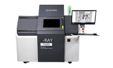
Two-dimensional X-ray and three-dimensional CT serve different inspection purposes.
| Evaluation factor | 2D X-ray inspection | 3D CT inspection |
|---|---|---|
| Image output | Two-dimensional projection | Reconstructed three-dimensional volume |
| Routine structural checks | Suitable for many visible internal features | Available when more detailed analysis is required |
| Overlapping copper layers | May create ambiguous projections | Can help separate features spatially |
| Complex internal geometry | Depends on viewing angle and contrast | Provides additional spatial information |
| Inspection time | Often faster for routine checks | Usually requires additional scanning and reconstruction |
| Best-fit application | Routine inspection and screening | Detailed analysis of complex internal structures |
A 2D system may be sufficient for straightforward structural checks, while CT can be beneficial when engineers need to investigate overlapping features or determine the spatial relationships between internal structures.
Seamark's offline X-ray inspection machine is a relevant option to evaluate for routine PCB inspection workflows. For more complex internal analysis, manufacturers can also consider industrial X-ray inspection.
The final selection should be based on sample testing, required inspection detail, throughput, and the types of defects that must be identified.
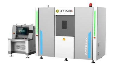
A repeatable inspection procedure helps manufacturers obtain consistent results and reduce uncertainty during defect evaluation.
Start by documenting the PCB stack-up, material types, via structures, and target defect categories. Next, select representative samples and establish image acquisition settings suitable for the required features.
Engineers should then compare inspection images with design information and verified reference samples. Suspicious findings should be classified according to documented criteria, with additional testing performed when X-ray images cannot establish the defect conclusively.
Finally, retain inspection images, sample identification, relevant settings, findings, and follow-up actions. This information supports traceability and helps quality teams compare results across production batches.
Yes. X-ray imaging can examine internal structures in multilayer rigid-flex PCBs. The visibility of individual features depends on board construction, material contrast, feature dimensions, and imaging settings.
Some larger structural abnormalities may be visible, but fine cracks or subtle copper plating defects may not be reliably detected. Cross-section analysis or electrical testing may be required.
Yes. Offline inspection can support sample evaluation, process troubleshooting, quality audits, and failure analysis when boards can be inspected at a separate workstation.
CT is worth evaluating when overlapping internal structures or complex geometries make two-dimensional images insufficient. Sample testing should confirm whether the additional spatial information provides meaningful value.
Manufacturers should provide PCB dimensions, layer-stack information, material types, target defects, required resolution, sample images, and expected inspection volume. These details help determine whether a proposed system is suitable.
Rigid-flex PCBs present unique inspection challenges because they combine multilayer conductive structures, flexible circuits, and complex internal interfaces. An X ray PCB inspection machine helps manufacturers examine selected internal features and investigate potential structural abnormalities without immediately damaging the sample.
The appropriate solution depends on board geometry, defect requirements, image quality, and inspection workflow. By combining industrial X ray inspection with representative sample testing, documented acceptance criteria, and complementary verification methods when necessary, manufacturers can establish a more reliable quality-control process. For applications requiring detailed internal analysis, CT-capable systems may provide additional spatial information, while offline inspection remains a practical option for many routine quality checks.
PREV
 EN
 es
 ko
 de
 it
 pt
 th
 ar
 pl
 vi
 tr
 ru