
QFN, DFN, and LGA packages are widely used in modern electronic assemblies because of their compact footprints and high connection density. However, their solder joints are often hidden beneath the component body, making visual inspection insufficient for evaluating certain connection defects. 3D industrial X-ray scanner technology can help manufacturers examine internal solder structures, identify potential assembly issues, and improve quality control.
For electronics manufacturers, selecting the right inspection method depends on package geometry, defect requirements, production volume, and quality standards. This guide explains the common defects found in QFN, DFN, and LGA assemblies, how X-ray imaging supports inspection, and when offline inspection or 3D computed tomography (CT) may be appropriate.
QFN (Quad Flat No-Lead), DFN (Dual Flat No-Lead), and LGA (Land Grid Array) packages use bottom-side electrical contacts rather than conventional visible leads. Once soldered to a printed circuit board (PCB), these connections are largely concealed by the component body.
This creates several inspection challenges:
Limited visual access: Optical inspection cannot directly view most solder joints beneath the package.
Hidden solder defects: Insufficient solder, bridging, voids, or incomplete connections may remain undetected by external inspection.
High connection density: Closely spaced pads increase the importance of identifying potential shorts and connection irregularities.
Difficult rework decisions: Manufacturers need reliable inspection evidence before deciding whether a component requires rework or further analysis.
X-ray inspection provides a non-destructive way to examine internal structures based on differences in X-ray absorption. It helps quality engineers evaluate solder distribution and identify suspicious features without immediately removing the component from the PCB.
Although these packages share similar inspection challenges, their geometries and soldering requirements differ. Defect interpretation should therefore consider the component design, PCB layout, and applicable acceptance criteria.
Voids are gas-filled spaces within a solder joint. Their significance depends on their size, distribution, location, and the function of the joint. Voids beneath a thermal pad may affect heat transfer, while voids in electrical connections may require evaluation against the product's quality requirements.
X-ray images can reveal void patterns and support quantitative analysis when the imaging system and software provide suitable measurement capabilities.
Solder bridging occurs when solder unintentionally connects adjacent conductive areas. In QFN and DFN assemblies, closely spaced bottom pads can make potential bridging difficult to inspect visually.
X-ray imaging can help identify suspicious connections, although overlapping structures in a two-dimensional image may complicate interpretation.
Insufficient solder can reduce joint integrity or contribute to an open electrical connection. An apparently missing or irregular solder region in an X-ray image may indicate a problem, but the image alone does not always establish electrical continuity.
Component displacement, inconsistent solder coverage, and asymmetric joint formation can indicate assembly process issues. Comparing images with known-good samples can help engineers distinguish acceptable variation from defects that require investigation.
X-ray inspection is most useful when image interpretation follows a defined inspection procedure rather than relying on appearance alone.
First, engineers should identify the package type, pad layout, solder geometry, and expected internal structure. Next, they should assess image contrast, magnification, resolution, and the possibility of overlapping features.
A two-dimensional X-ray image projects internal structures onto a single plane. When several features overlap, it may be difficult to determine their exact depth or spatial relationship.
A 3D industrial x ray scanner or CT-capable inspection system can provide additional spatial information by reconstructing internal structures from multiple projections. This can be valuable when two-dimensional imaging cannot sufficiently separate overlapping features or when detailed internal analysis is required.
However, 3D imaging is not automatically necessary for every assembly. The appropriate method depends on defect size, material composition, component geometry, inspection throughput, and the level of evidence required.
X-ray images should also be interpreted alongside other quality data when appropriate. Electrical testing, automated optical inspection, cross-section analysis, and established reliability tests may be needed to confirm specific failure mechanisms.
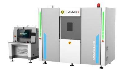
Choosing between two-dimensional X-ray and three-dimensional CT requires balancing inspection requirements against operational costs and production constraints.
| Evaluation factor | 2D X-ray inspection | 3D CT inspection |
|---|---|---|
| Image output | Two-dimensional projection | Three-dimensional reconstruction |
| Inspection speed | Often suitable for faster routine inspection | Typically requires more acquisition and reconstruction time |
| Overlapping structures | May be difficult to distinguish | Can provide additional spatial separation |
| Defect analysis | Suitable for many visible internal features | Useful for more complex internal geometry |
| Equipment considerations | Depends on resolution, automation, and configuration | Depends on reconstruction quality, scan time, and system capability |
| Best-fit application | Routine inspection and screening | Detailed internal analysis when 2D results are insufficient |
For high-volume electronics manufacturing, offline inspection can be a practical option when selected boards or samples need to be examined outside the main production line. It allows engineers to investigate quality issues, verify process changes, and analyze suspicious solder joints without necessarily requiring an inline inspection installation.
For more complex internal structures, a CT-capable system may offer additional analytical value. Manufacturers should evaluate both methods using representative samples rather than relying exclusively on advertised specifications.
A repeatable inspection process requires clear acceptance rules and appropriate reference samples.
Before selecting equipment, manufacturers should establish the following:
Define target defects. Identify whether the primary concern is voiding, bridging, misalignment, insufficient solder, or another internal feature.
Prepare representative samples. Include known-good assemblies and samples containing verified defects wherever available.
Set image quality requirements. Evaluate whether the system can resolve the smallest features relevant to the inspection task.
Establish acceptance criteria. Apply customer specifications, component requirements, and applicable industry standards instead of using universal thresholds for every package.
Validate repeatability. Check whether repeated inspections produce consistent results under defined conditions.
Document inspection results. Record images, defect classifications, reference criteria, and follow-up actions to support traceability.
Manufacturers evaluating an offline inspection solution should also consider sample handling, operator workflow, inspection time, image storage, and compatibility with existing quality management procedures.
Yes. X-ray imaging can reveal voids within solder joints when image quality and inspection settings are suitable. Their acceptability depends on their size, location, distribution, and the applicable product criteria.
No. Two-dimensional X-ray may be sufficient for routine inspection and many common solder defects. CT is more appropriate when additional spatial information is necessary to resolve overlapping structures or investigate complex internal features.
No. X-ray primarily provides structural information. Electrical testing or other validation methods may be required to confirm continuity and functional performance.
Offline inspection is suitable when inspection can take place at a separate workstation, such as during sample evaluation, process troubleshooting, failure analysis, or quality audits. Inline inspection may be preferable when automated inspection must be integrated directly into production flow.
Buyers should provide package types, PCB dimensions, target defects, required resolution, inspection volume, sample images if available, and applicable acceptance criteria. Representative samples enable a more meaningful equipment evaluation.
QFN, DFN, and LGA packages require careful inspection because their solder connections are hidden beneath the component body. X-ray technology helps manufacturers examine internal solder structures, identify suspicious defects, and strengthen electronics quality control.
The best solution depends on the package design, defect requirements, inspection speed, and available quality standards. While 2D X-ray can address many routine inspection needs, a 3D industrial x ray scanner may provide additional insight when complex internal structures require more detailed analysis. By validating equipment with representative samples and documented acceptance criteria, manufacturers can make more informed inspection decisions and select an appropriate offline inspection or CT-based solution.
 EN
 es
 ko
 de
 it
 pt
 th
 ar
 pl
 vi
 tr
 ru